Semiconductor Metrology
Ellipsometry, Lithography, and Photoresist Development
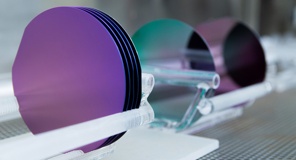
Top quality, high-production yields are critical to meeting market demand for semiconductor wafers. Wafer metrology tools help semiconductor manufacturers design and fabricate high performance integrated circuits (ICs) with less defects, enabling them to scale to meet rising demands. The faster you can characterize and measure thin films, linewidths, pattern flaws, and other potential defects, the faster you can address the issue and reduce costly downtime.
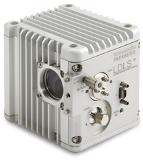
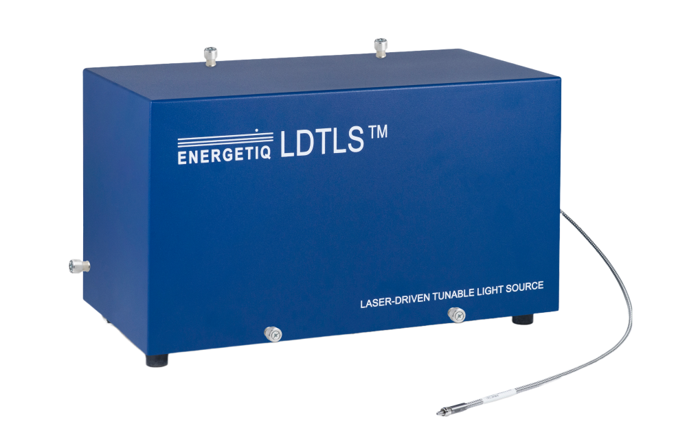
Broad wavelength, high spectral radiance light sources illuminate these anomalies with speed and accuracy. The unique principle of operation of the LDLS®, with its small plasma size and high spatial stability, enables high throughput measurements ideal for volume production environments.
- Thin film and materials characterization
- Defect review
- Analysis
- Classification